This article is also published on many digital book stores for the benefit of eBook readers. The new edition is DRM-free and can be read whilst offline. Furthermore, it's updated at the same pace as the website.
You can find the eBook at Amazon Kindle, Apple Books, Kobo and other stores. The profits contribute towards the improvement of current articles and the development of future ones.
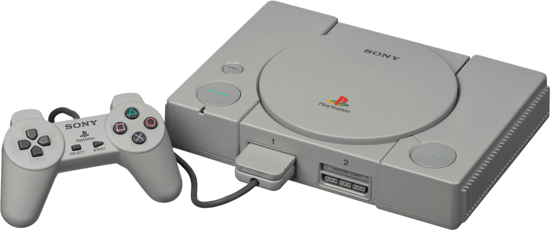
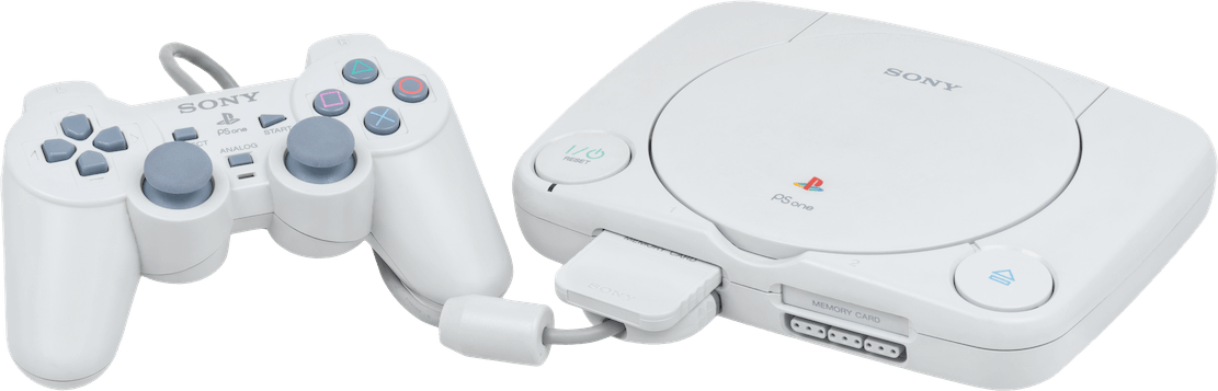
The original PlayStation. Released on 03/12/1994 in Japan, 09/09/1995 in North America, 29/09/1995 in Europe.The PS One (slim revision). Released on 07/07/2000 in Japan, 19/09/2000 in North America, 29/09/2000 in Europe. This is what you get after cramming so many custom ICs into a single one.
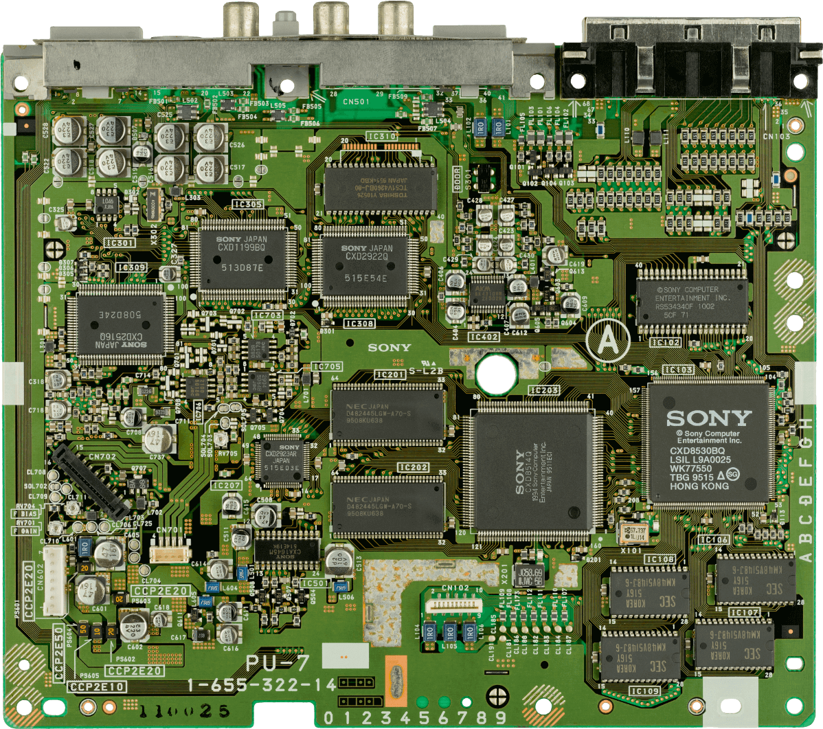
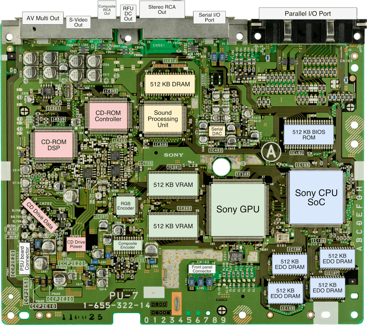
Motherboard Showing model 'SCPH-1000'. Remaining chips are fitted on the back. Later models included SG-RAM instead of VRAM and removed most of the external I/O and video outs.Motherboard with important parts labelled
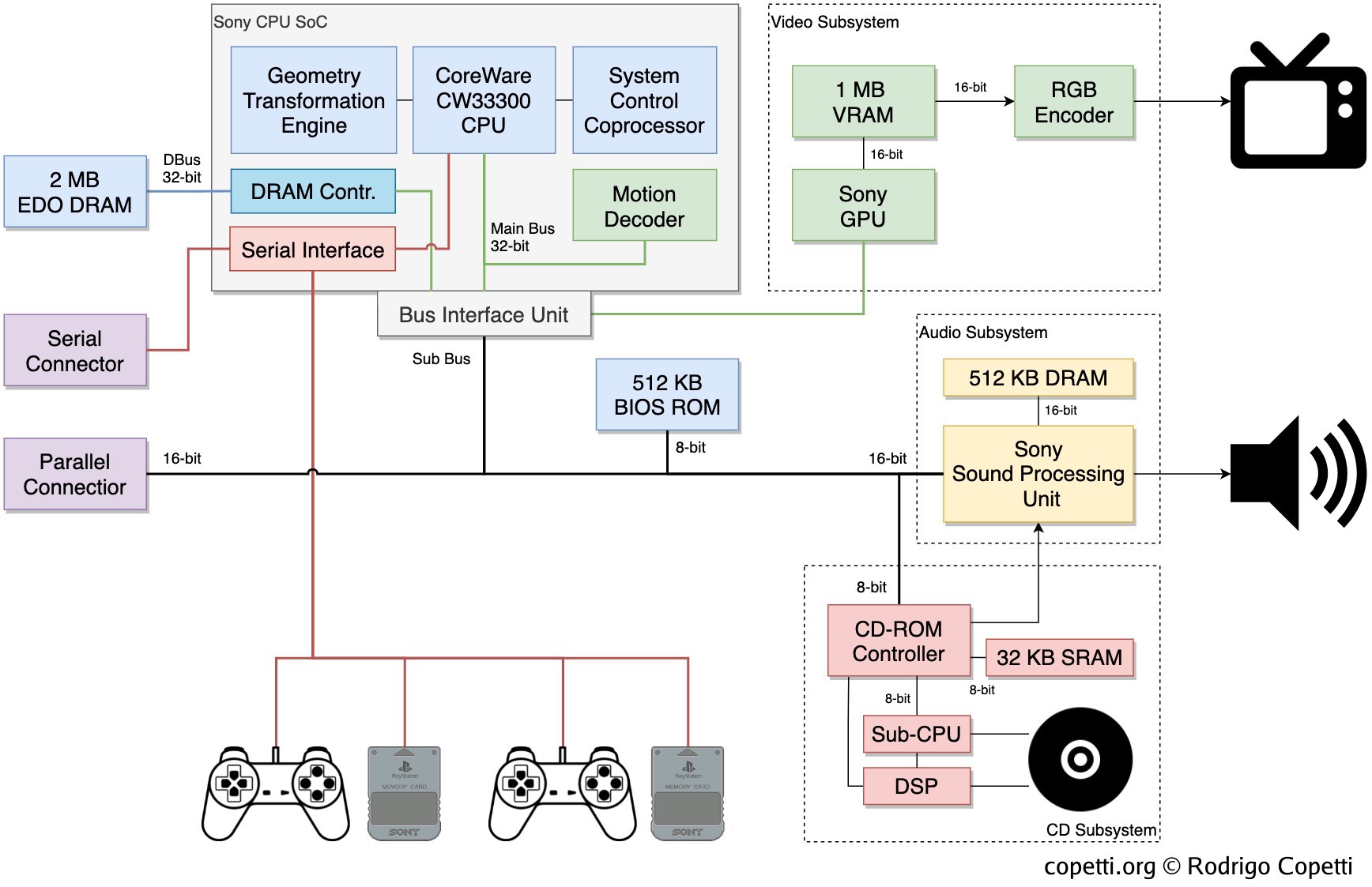
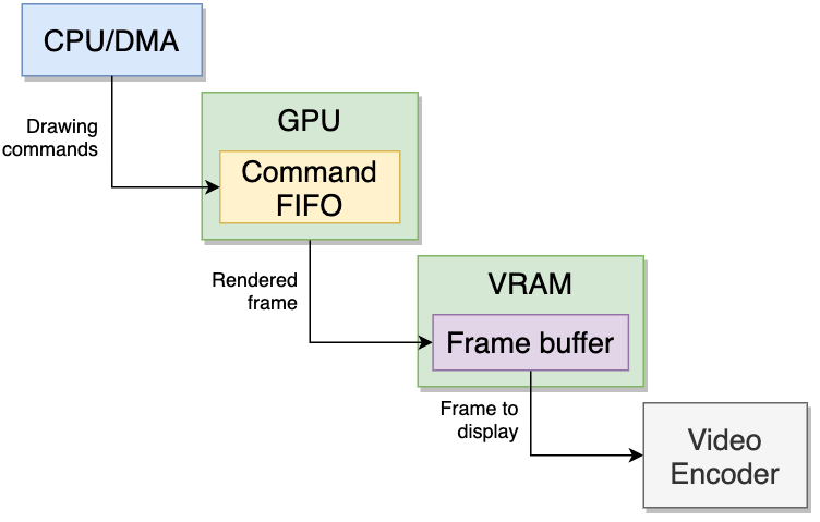
DiagramMain architecture diagram The Bus Interface Unit is also connected to special ports of the GPU and SPU.
A quick introduction
Sony knew that 3D hardware could get very messy to develop for. Thus, their debuting console will keep its design simple and practical… Although this may come with a cost!
CPU
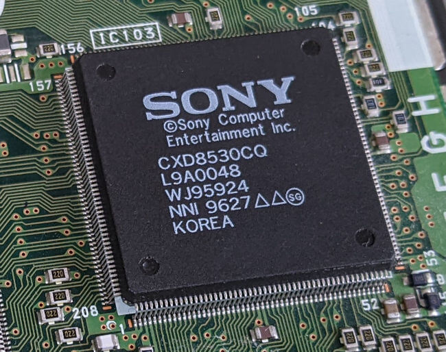
This section dissects the Sony CXD8530BQ, one of the two big chips this console houses. It’s what we would call a ‘System-on-Chip’ in today’s world.
The origins
The main processor is one of those ‘x designed by y, based on z and second-sourced from w’ which is a bit dense to summarise in a few sentences, so why don’t we start with some historical context?
The early nineties were marked by a change in the fates of many popular CPUs. The once-leading 8-bit CPUs, such as the Z80 and 6502, were already out of spotlight and Motorola’s famous 68000, along with other 16-bit designs that enjoyed success in the late 80s, had become candidates for replacement. Even at this time in the PC world, Tanenbaum, in his celebrated debate with Torvalds, gave Intel’s x86 architecture only five more years until its demise from the home market.
At first, it may look as if technological development had hit a wall at this point. But in reality, there was a new wave of relatively unknown CPUs making their way into mainstream devices. Many of these designs had originated in academia, and so existed to prove particular sets of design ideas. Examples of novel CPUs of that era included:
MIPS: Adopted by Silicon Graphics Incorporated (targeting graphics workstations).
PowerPC: Adopted by Apple (targeting desktop publishing).
SPARC: Created by Sun Microsystems (targeting servers and business workstations).
ARM: Created by Acorn (initially targeting the consumer market and then, PDAs and cell phones).
… and many more ‘microcontroller’ chips yet to be finalised or adopted by any industry, such as Hitachi’s SH or NEC’s V810. To their surprise, these were subsequently selected for the Sega Saturn and the Nintendo Virtual Boy, respectively.
All of these processors had something in common: They followed the Reduced Instruction Set Computer (RISC) discipline, which radically shifted how these chips had to be designed and programmed. One rule of RISC CPUs dictated that a single instruction can’t mix memory with register operations, allowing hardware designers to simplify the circuitry that executes instructions… and then enhance it with parallelism techniques.
MIPS Computer Systems originated from the eagerness of its founders (Stanford faculty) to turn their research into physical processors, something that Silicon Valley-based venture capitalists in the 80s were also anxious to invest in [1]. Their debuting CPU, the ‘MIPS R2000’, is considered the first commercial CPU to incorporate a RISC design; and it found a space in many UNIX workstations.
However, it wasn’t until 1987 that MIPS’ chips became a topic of conversation, all due to being adopted (and later acquired) by Silicon Graphics Incorporated (SGI) to power their equipment. SGI was an influential innovator in the computer graphics market, especially with the development of hardware-accelerated vertex pipelines, whose task was originally carried out by software (within the CPU). After the acquisition, SGI had a leading position in both CPU and graphics sectors.
Before the development of the PlayStation, MIPS switched to a business model based on IP licensing, where their CPU designs would be sold in the form of licenses, and licensees were then free to customise and manufacture it. Part of their offerings included the R3000A CPU, albeit within their low-end catalogue. Consequently, while the R3000A wasn’t associated with the flagship lineup (unlike the R4000, which others would later choose), it was an attractive investment in terms of cost.
Sony designed their audio and graphics chips in-house, but they still needed the leading chip that could drive those two. The selected CPU had to be powerful enough to show off the impressive capabilities of Sony’s chips, but also affordable to keep the console at a competitive price.
At the same time, LSI Logic (a semiconductor manufacturer) was a MIPS licensee that provided a ‘build-your-own’ CPU program for businesses. This service was referred to as CoreWare and it enabled clients to build their own CPU packages by choosing a series of building blocks [2]. Part of the CoreWare library included the ‘CW33300’ block, a CPU core derived from the LSI LR33300, an off-the-shelf CPU chip that LSI also commercialised.
Now, where am I going with all this? It turns out LSI’s LR33300 and CW33300 are a binary-compatible version of the MIPS R3000A family. Their architectures slightly differ in some areas but the programming interface (MIPS I ISA) remains the same.
In the end, Sony commissioned LSI to build their CPU package. They chose the CW33000, changed some bits and combined it with other blocks to form the chip you find on the PlayStation’s motherboard.
The SoC chip on the PlayStation’s motherboard, where the MIPS R3000A-based core resides.
The resulting CPU core runs at 33.87 MHz and features:
The MIPS I ISA: The first version of the MIPS instruction set. Among many things, words are 32-bit long and the instruction set includes multiplication and division instructions.
32 general-purpose registers and 2 multiplication/division registers: These are 32-bit as well. One general-purpose register is always zero (R0), which is common in RISC processors.
32-bit data bus: In the PS1, the data bus forks into two buses.
Main Bus (32-bit) → Connects the MDEC and GPU.
Sub Bus (16/8-bit) → Connects the rest of the chips and I/O. This bus is bridged by the Bus Interface Unit, which also enables access to special ports of the GPU and SPU.
32-bit address bus: Up to 4 GB of physical memory (i.e. RAM, memory-mapped I/O, etc) can be accessed.
5-stage pipeline: Up to five instructions can be executed simultaneously (a detailed explanation can be found in a previous article).
4 KB of instruction cache: It can be ‘isolated’ as well, allowing the program to manipulate the instruction cache directly.
Oddly, there is no data cache. The 1 KB of memory normally used for the data cache is mapped to a fixed address [3]. This area is also called Scratchpad (fast SRAM).
To do something meaningful, Sony provided 2 MB of RAM for general-purpose use. Curiously enough, they fitted Extended Data Out (EDO) chips on the motherboard. These are slightly more efficient than typical DRAM, obtaining lower latency.
Taking over the CPU
At some point, any subsystem (graphics, audio or CD) will require large chunks of data at a fast rate. However, the CPU will not always be able to keep up with the demand.
For this reason, the CD-ROM Controller, MDEC, GPU, SPU and the Parallel port have access to an exclusive DMA controller whenever they require it. DMA takes control of the main bus and performs a data transfer. The resulting rate is a lot faster than relying on the CPU, though the latter is still needed to set up a DMA transfer.
Also, bear in mind that once DMA kicks in, the CPU can’t access the main bus. This means the CPU will be idling unless it’s got something in Scratchpad to keep it busy!
Complementing the core
Like other MIPS R3000-based CPUs, the CW33000 supports configurations with up to four coprocessors, Sony customised it with three:
Identified as ‘CP0’, the System Control Coprocessor is a common block found on MIPS CPUs. In R3000-based systems, like this one, the CP0 controls how the cache is implemented. Thus, enabling direct access to data cache (in the form of ‘Scratchpad’) and instruction cache (using ‘cache isolation’). The control coprocessor is also responsible for handling interrupts, exceptions and breakpoints, the latter is useful during debugging.
Wait, shouldn’t co-processors only expand CPU functions? Why is CP0 tightly coupled to the CPU?
Indeed, R3000 cores depend on the system control coprocessor to be able to make use of many components, but whether this should be ‘legal’ or not comes down to the interpretation of the word ‘co-processor’. According to MIPS, a co-processor is not strictly an optional part of the CPU, it may also command the CPU’s surroundings (cache, interrupts, etc). Hence, a co-processor can be an integral part of the system. This is just something to bear in mind while talking about MIPS-related systems.
Later R4000-based systems incorporated a Memory Management Unit (MMU) and a Translation Lookaside Buffer (TLB) into this block, thereby increasing its capabilities and taking up new roles.
The ‘CP2’ or Geometry Transformation Engine (GTE) is a special math processor that accelerates vector and matrix calculations.
While only operating fixed-point types, it still provides useful operations for 3D graphics such as:
Matrix or vector multiplication and addition; and vector square.
Perspective transformation (used for 3D projections).
Outer product of two or three vectors (the latter is used for clipping).
Many interpolation functions that use different parameters.
Depth Cueing and colour value from a light source (used for lighting and colour operations).
Z/depth average (I suspect this is for the ‘ordering table’, more details in the ‘Graphics’ section).
You don’t have to remember all these to follow the rest of the article! Just keep in mind that the GTE will be taking care of the first stages of the graphics pipeline, such as 3D projection, lighting and clipping. This will help to generate the required data that will be sent to the GPU for rendering.
The Motion Decoder, also called ‘MDEC’ or ‘Macroblock Decoder’, is another processor living next to the CPU. This time, it decompresses ‘Macroblocks’ into a format the GPU can understand. A Macroblock is a data structure that houses a picture with similar encoding to JPEG.
The MDEC decompresses bitmaps made of 8x8 24 bpp pixels at a time. Walker’s programming guide states the MDEC can compute 9,000 macroblocks per second. This would allow to stream a 320x240 px full-motion video (FMV) at 30 frames per second.
DMA is used to send compressed data through CD-ROM → RAM → MDEC. The same path is taken in the opposite direction, though in this case, the destination is VRAM.
While this component is sitting inside the SoC and shares the same data bus, it’s not a MIPS co-processor, so the CPU/DMA access it through the memory map (as opposed to intercepting instructions).
For more info about the MDEC unit, I suggest checking out Sabin’s [4] and Czekański’s [5] resources.
So far, we got a ‘CP0’ and a ‘CP2’, but where’s the ‘CP1’? Well, that’s reserved for a Floating Point Unit (FPU) and I’m afraid Sony didn’t provide one. This doesn’t mean the CPU can’t perform arithmetic with decimal numbers, it just won’t be fast enough (software-emulated FPU) or too precise (fixed-point arithmetic instead).
Game logic (involving physics, collision detection, etc) still can get around with fixed-point arithmetic. Fixed-point encoding stores decimal numbers with an immutable number of decimal places. This implies a loss in precision after certain operations, but remember, this is a video-game console, not a professional flight simulator. Hence, the precision-performance trade-off is somewhat feasible.
By the way, sometimes I mix up ‘fixed-point’, ‘floating-point’, ‘decimal’ and ‘integer’ number types (hopefully not anymore!). If you feel the same, I recommend taking a look at Gabriel Ivancescu’s quick summary [6] to quickly refresh those concepts.
Delay galore
As we’ve seen before, the CW33300 is a pipelined processor, meaning that it queues up multiple instructions and executes them in parallel at different stages. This hugely improves instruction throughput, but if it’s not controlled properly, it can lead to pipeline hazards, resulting in computational errors.
Control hazards: Instructions may get executed when they shouldn’t be
Data hazards: Instructions may operate with outdated data before it’s been updated.
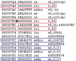
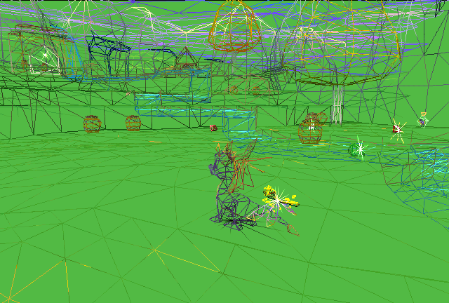
Instructions from ‘Spyro The Dragon’ visualised on the NO$PSX debugger. Notice how LW (load word from memory), JAL (jump and link) and BNE (branch on not equal) are followed by a delay slot to prevent hazards. Marked in red are fillers (useless instructions). Marked in blue perform meaningful operations.
Consequently, MIPS I CPUs exhibit the following behaviour:
Any instruction following a ‘branch’ or ‘jump’ type opcode is executed unconditionally: Thus, developers have to manually fill the pipeline with modest instructions (such as calculate 0 plus 0) after the branch or jump to mitigate the hazard. These fillers are called branch delay slots.
Modern CPUs converted this phenomenon into an advantage: Branch prediction. By adding extra circuitry to detect the hazard, the CPU discards the new computations if the branch/jump condition isn’t met. But if it did, then the CPU has saved some time.
‘Load’ instructions don’t stall the pipeline until the retrieved data is made available: The second stage of the pipeline (called RD or ‘Read and Decode’) gathers the operators [8], which will be used to perform a computation at the third stage (ALU). The fourth stage (MEM, from ‘access MEMory’) looks for data in memory (i.e. main RAM, CD reader, etc). Now, here’s the problem: by the time a load instruction gathered the data from outside, the following instruction had already fetched the operators. This means that an instruction depending on the values of the previous load instruction requires a filler in-between, so the correct operators can be fetched on time.
As we can see from the example, some delay slots are filled with meaningful instructions, which perform computations that are not affected by the hazard. Hence, delay slots don’t always imply a waste of cycles.
Having explained this, you may be wondering why a processor with these kinds of flaws could ever be commercialised. Well, one philosophy about RISC is that the burden of CPU programming is shifted from the developer to the compiler. MIPS, in particular, prioritised the production of good quality compilers (including assemblers) to accompany their new CPUs [9]. Hence, developers could use a higher-level language (for instance, C) while the compiler dealt with the hazards (by re-arranging instructions to fill in slots; or adding useless fillers as a last measure). So, all in all, while I don’t find it pleasant to see a CPU being filled with bubbles, I think MIPS tackled this in a very clever way.
Graphics
To recap, a large part of the graphics pipeline is carried out by the GTE. This includes perspective transformation (which projects the 3D space onto a 2D plane using the camera’s perspective) and lighting. The processed data is then sent to Sony’s proprietary GPU for rendering.
Organising the content
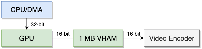
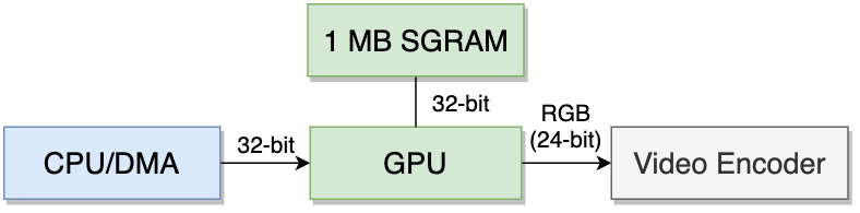
The system features 1 MB of VRAM that will be used to store the frame buffer, textures and other resources the GPU will require to render the scene. The CPU can fill this area using DMA.
The type of chip fitted (VRAM) is dual-ported, like the Virtual Boy’s. VRAM uses two 16-bit buses, which enables concurrent access between the CPU/DMA/GPU and the Video encoder.
Memory layout using VRAM.Memory layout using SGRAM.
Though in later revisions of this console, Sony switched to SGRAM chips (the single-ported option using an individual 32-bit data bus). Boo!… Well, to be fair, each one comes with its pros and cons. One thing for sure is that due to the timing differences, later games (such as Jet Moto 3) will display glitched graphics when ran on VRAM-based systems. If you want to know the details, Martin Korth’s ‘Nocash PSX Specifications’ document the different timings and such [10].
Drawing the scene
If you’ve been reading the Sega Saturn article, let me tell you that the design of this GPU a lot simpler!
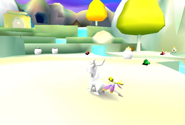
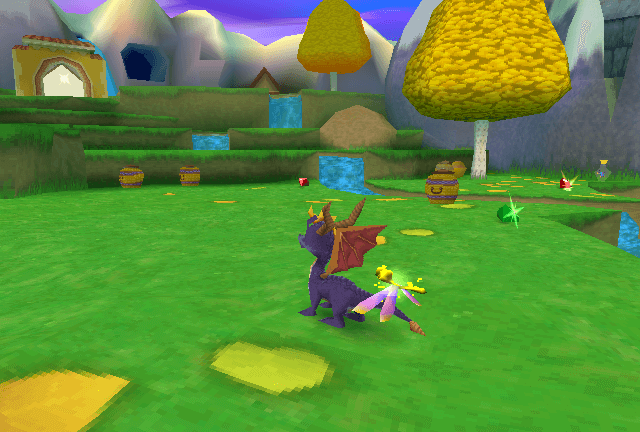
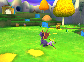
Now, to show how a scene is drawn, I’ll mainly use Insomniac’s Spyro: Year of the Dragon as an example. Please bear in mind that the internal resolution of this game is too cramped (292x217 px), preventing me from clearly dissecting it at each stage, so I’ve upscaled it a bit for demonstration purposes.
Here is a sample at original scale if you are curious.
To start with, the CPU sends geometry data (vertices) to the GPU by filling its internal 64-byte FIFO buffer with commands (up to three). Essentially, a command states how and where to draw one primitive.
Once the geometry is received, clipping is applied to skip operations over unseen polygons (residing outside the camera’s viewport).
The location of the primitive is stated with an X/Y coordinate system pointing to the frame buffer. The PS1’s GPU employs an integer coordinate model, where each coordinate corresponds to the centre point of a pixel (called sampling point). In other words, there are no fractional coordinates.
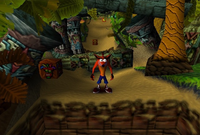
Crash Bandicoot (1996). This game used pre-ordered geometry to gain performance [11]. Hence, its camera only moves backwards or forward.
Just like the competition, the PS1 doesn’t include any hardware feature that solves the visibility problem. Nonetheless, the GPU handles sorted polygons by providing an ordering table: A dedicated table where each entry is indexed using a depth value (also called ‘Z-value’) and contains the address where the GPU command resides [12].
The CPU needs to manually sort the polygons first, and then reference them in the correct entry of the table. Finally, the CPU orders DMA to send the table to the GPU. This process will enable the GPU to render the geometry in the correct order.
Multiple DMA functions are also provided to assist both CPU and GPU with the creation and traversal of this table.
Once the commands are decoded by the GPU, it’s time to convert the geometry received (vertices) into pixels. This will enable the system to apply texture mapping, effects and ultimately display it on a two-dimensional panel (your TV or monitor). To do this, the GPU allocates a pixel matrix that is used as a working area, this is called a frame buffer. Compared to the more complex Sega Saturn, the GPU only needs a single frame buffer.
The GPU uses triangles as primitives to form 3D models. Being the only available primitive means that backgrounds and foregrounds make no difference in terms of composition (both are made of triangles). 2D games inherit the same nature: They are just two triangles joined to form a quadrangle (though the GPU provides routines for constructing sprites automatically).
The rasteriser is the unit in charge of converting vectors into triangles; and then into pixels. This is done by:
Grabbing each three-point vertex and calculating the edges. This forms a triangle.
Analysing the area of the triangle to identify which pixels of the frame buffer they occupy. Any section of the triangle covering the sampling point is turned into a pixel.
The generated pixels are not written into the frame buffer right away. Instead, they are sent to the next stages of the pipeline for further processing, which we’ll see in the following paragraphs.
In order to apply lighting effects over these polygons, the GPU provides two algorithms:
Flat shading: Each primitive has a constant light level.
Gouraud shading: Each primitive’s vertex embeds its own light level. Then, the brightness between each point is automatically interpolated.
As you can imagine, the results are more realistic. On the other hand, this algorithm is not available for sprites.
The reason for having this choice comes down to the fact that flat shading fills ~2.5 times more polygons per second than Gouraud, so it’s important to optimise which polygons need a more realistic shading than others.
Finally, shaded surfaces are blended with textures (2D bitmaps) to produce the final result.
The GPU performs inverse texture mapping, where the GPU traverses each rasterised pixel and looks for its corresponding pixel in the texture map (called texel). Texels are calculated by linearly interpolating the texture map (found in VRAM) to conform to the shape of the polygon. The routine used for interpolation is called Affine Texture Mapping, this technique only operates using 2D coordinates (X/Y values) while discarding the third coordinate (Z/depth) used for perspective.
Because texture maps rarely have the exact dimension of the rasterised polygon, aliasing (incorrect results) may appear. This is manifested with unwanted distortions, such as missing or enlarged texels. To remedy this, sophisticated GPUs employ texture filtering to smooth out (interpolate) sudden colour changes. Now, The PS1’s GPU doesn’t implement any filter, so it resorts to an algorithm named nearest neighbour to correct scales without smoothing out the results. This is very fast (and cheap) but it also explains why textured models may look ‘blocky’.
The unit also includes the following effects available to use:
Semi-Transparency: Simulates light passing through multiple textures.
Dithering: Soften sudden changes in colour while adhering to the same colour palette.
It’s worth mentioning that the PS1 happened to excel at those effects!
Once finished, the GPU writes the pixels into the frame buffer area in VRAM, which is in turn picked up by the video encoder and broadcast to the screen.
Designs
Let’s take a break now from all this theory. Here are some examples of game characters designed from the ground up for the 3D era, they are interactive so I encourage you to check them out!
Wireframe
Surface
Textured
Tap to enable interaction
Spyro the Dragon (1998). 413 triangles.
Wireframe
Surface
Textured
Tap to enable interaction
Crash Bandicoot (1996). 732 triangles.
Playing with VRAM
With the available amount of VRAM (1 whole megabyte), one could allocate a massive frame buffer of 1024×512 pixels with 16-bit colours or a realistic one of 960×512 pixels with 24-bit colours - allowing one to draw the best frames any game has ever shown… This sounds pretty impressive, right? Well, it does raise a couple of issues, for instance:
Those dimensions will have to be rescaled to follow a standardised definition (i.e. 480 NTSC, 576 PAL) so the video encoder can broadcast it to consumer TVs.
How is the GPU going to be able to draw anything decent if there isn’t any space left for the rest of the materials (i.e. textures, colour tables, etc)?
The PS1’s GPU can only draw frame buffers with up to 640×480 pixels and 16 bpp colours.
All right, so let’s have a 16 bpp 640x480 buffer instead, which leaves 424 KB of VRAM for materials. So far so good? Again, such resolution may be fine on CRT monitors, but not particularly noticeable on those 90s TVs everyone had in their homes. Then, is there any way to optimise the frame-buffer? Introducing adjustable frame-buffers.
VRAM visualisation on the NO$PSX debugger. You can spot the dual-frame buffer, along with textures (to be translated using a colour-lookup table, also stored there).
In essence, instead of wasting valuable VRAM by using ‘unappreciated’ resolutions, this console’s GPU allows decreasing the dimensions of the frame buffer to effectively increment the space available for other resources. In ‘Gears Episode 2’ [13], Halkun shows a setup that divides the 640x480 frame buffer into two 320x480 ones, and then relies on a technique called page-flipping to render multiple scenes at the same time.
Page-flipping consists of switching the location of the frame for display between the two available whenever the game wants it, allowing the game to render one scene while displaying another. Thus, hiding any flickering effect and improving loading times (something that the player will certainly appreciate!).
Overall, Halkun’s layout only consumes 600 KB of VRAM. The rest (424 KB) can be used to store colour lookup tables and textures that, combined with 2 KB of texture cache available, result in a very convenient and efficient setup.
Finally, it is worth mentioning that VRAM can be mapped using multiple colour depths simultaneously, meaning that programmers can allocate a 16 bpp frame buffer next to 24 bpp bitmaps (used by FMV frames, for instance). This is another feature facilitating further optimisation of space.
Secrets and Limitations
Whereas the PS1 had a very simple and suitable architecture, problems ended up arising anyway. Surprisingly, certain issues were tackled with very clever workarounds!
Square Soft’s Final Fantasy VIII (1999). Textures jiggle a bit while they move.
The routines used for handling geometry and applying textures are known to carry some inaccuracies.
Firstly, the rasteriser only handles pixel units: While vertex coordinates are integers, the calculated triangle edges may only occupy a fraction of a pixel. However, the rasteriser will only draw the pixel if the triangle area covers the pixel’s sampling point, and it won’t keep track of the fraction occupied[14]. This brings up some problems:
External edges of models make sudden jumps when moved slightly.
Triangles within a mesh (sharing the same vertices and edges) will be ‘fighting’ to draw over the same pixels. With the ordering table, the GPU will draw following a ‘last-come first served’ basis, which can lead to triangle intersections flickering or overlapping when moved slightly.
This is commonly tackled by implementing sub-pixel resolution, from which the rasteriser keeps track of the fractions of pixels occupied by each triangle area [15]. Consequently, anti-aliasing methods can then be added to soften jagged edges or sudden changes in colour.
Moving on, the ordering table puts the burden on the developer/program to show the geometry in the right order. In some cases, the calculations implemented rely on too many approximations to gain performance. This may result in flickering or occluded surfaces that should have been displayed.
Furthermore, setting a low-resolution frame buffer may amplify all these aliasing issues.
Finally, as you know, affine transformations have no sense of depth, which may confuse the user’s perception when the camera is close to the model and is positioned perpendicular to the viewer [16]. The effect is also referred to as texture warping. Hence, some games resorted to tessellation (dividing a big polygon into smaller ones) to reduce distortion, others just swapped textures in favour of solid colours. In general, a GPU ultimately tackles this issue by implementing perspective correction, which interpolates textures using the depth value.
If you check other technical channels or forums, you’ll find alternative explanations about the PS1’s wobbling/warping/distorted effects. While some of them will coincide with what I explained before, others will argue differently. So, I’d like to give my opinion on why the following statements are not accurate:
Models/textures wobble due to lack of FPU
An FPU doesn’t dictate whether a computer can operate or not fractional numbers. The PS1, like any other computer without an FPU, can still perform fixed-point arithmetic. Furthermore, using software emulation, floating-point numbers can also be computed (just slower). To sum up, FPUs are just accelerators, do not confuse them with an ALU (the critical portion of a CPU that performs arithmetic) or decimal numbers.
Models/textures wobble due to the GPU’s integer coordinate system
Employing integer coordinates is a common approach to make calculations less expensive in the GPU. It’s the fact of not employing sub-pixel resolution that turns this into a visible problem. To sum up, anti-aliasing could be applied to smooth out sudden changes of colours if the rasteriser kept count of the pixel’s fraction occupied by the triangle.
Textures warp due to lack of mipmapping
GPUs that implement inverse texture mapping such as this one, are subject to a measurement error called ‘undersampling’ (one pixel is mapped to multiple texels). Thus, this creates aliasing (wrong results). The behaviour is noticeable when rendering geometry far away from the camera. To remedy this, modern texture mappers apply ‘trilinear filtering’, which softens texels using the same texture stored at different scales (mipmaps) and does some interpolation in-between. To sum up, mipmapping is an approach to solve aliasing. It’s affine texture mapping (with its lack of perspective correction) that interpolates textures on three-point surfaces without taking into account the depth. Hence, the ‘warping’ effect.
Models/textures flicker due to lack of Z-buffering
A GPU with Z-buffer solves the Visible surfaces determination problem at a hardware level. The PS1 relies on an ordering table, meaning developers are in charge of determining what geometry is in front of others. To sum up, any model exhibiting flickering triangles is caused by the sorting routines (software), so it’s remedied on the same software.
Square Soft’s Final Fantasy VII (1997). A scene with Pre-rendered background. The way models interact and move is essential to trick the user’s perception.
Let’s mention a ‘positive’ feature now for a change…
If a game strived for a more realistic scenery than the GPU could provide, one available option was to stack two triangles and use the Motion Decoder to feed pre-rendered cinematic on them. FMV video could weigh a lot of space, luckily the CD-ROM was prepared for this.
Some games relied on it specifically for composing backgrounds and, honestly, it was quite convincing to see them on a CRT TV, obviously modern emulators with upscaling capabilities will tell on very quickly.
The first revision of this console carries a surprising amount of video signals with the following ports:
RFU DC: This one got removed pretty quickly, it was meant to be connected to an RF modulator.
RCA: Provides composite video.
S-Video: Provides Luma + Sync (combined) and Chroma.
AV Multi Out: Provides all the previous signals, except RFU, plus RGB and a 5+ Volts line.
Later revisions of the console removed these ports and at the end, only ‘AV Multi Out’ was left.
Audio
Sony’s signature Sound Processing Unit (SPU) takes care of this. This chip supports the enormous amount of 24 channels of 16-bit ADPCM samples (a more efficient version of the well-known PCM sampling) with a sampling rate of 44.1 kHz (Audio CD quality).
This chip also provides the following capabilities:
Pitch modulation: As the name suggests, games can automatically alter the pitch of their samples instead of needing to store extra ones. This is useful for music sequencing.
Frequency modulation: Voices can be assigned to alter the frequency of others. Comparable to FM synthesis.
ADSR Envelope: These are a set of properties available for amplitude modulation.
Looping: Instructs the system to play a piece of audio repeatedly.
Digital reverb: Simulates the sample being played within a specific atmosphere to immerse the player.
512 KB of DRAM (called ‘Sound RAM’) are provided as audio buffer. This memory is accessible from the CPU (only through DMA) and the CD controller. Although games only have 508 KB available to store samples, the rest is reserved by the SPU to process Audio CD music. This amount is reduced even further if reverb is activated.
The CD controller is also able to send samples directly to the audio mixer without going through the audio buffer or requiring CPU intervention. Samples can also be compressed using the ‘XA’ encoding, which the SPU can decode on the fly.
The streaming era
Similarly to the Saturn, games are no longer dependent on music sequencing or pre-defined waveforms, and thanks to the amount of storage available on the CD-ROM medium, developers can store fully produced samples and just stream them to the audio chip.
I/O
There are two I/O ports (Serial and Parallel) available for add-ons. However, these were removed in later revisions of the console due to lack of adoption and the fact that they could potentially be used to crack the copy protection system.
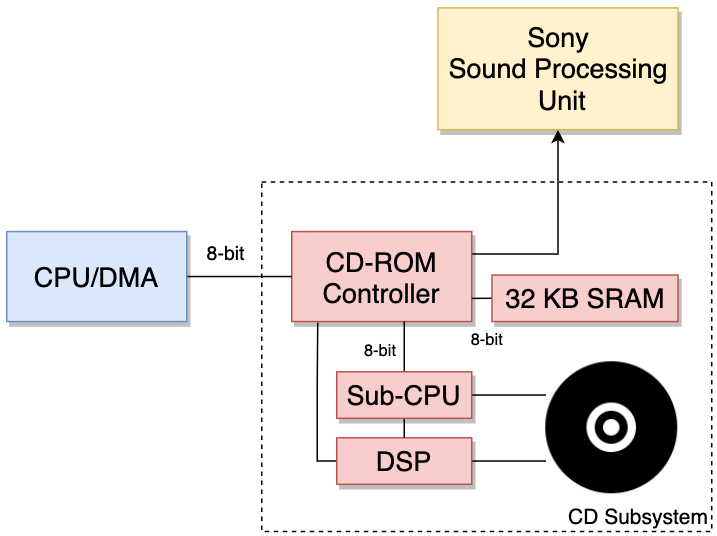
CD subsystem
The block controlling the CD drive is an interesting area, you can imagine it as a separate computer living inside the PlayStation.
CD Subsystem layout.
This subsystem is composed of:
A DSP: controls the motor and laser, and processes the RF signal coming from the laser.
A Sub-CPU: A CPU package made of a Motorola 68HC05 microcontroller, 512 B of RAM and 16 KB of ROM[17]. In a nutshell, the Sub-CPU runs a local program stored in ROM and controls the DSP. The Sub-CPU program implements copy-protection measures and they are enforced whether the main CPU ‘likes it or not’.
A CD Controller: This is the middle-man between the CD subsystem and the rest of the console, receiving commands from main CPU (in a FIFO manner) and triggering interrupts after certain events. As a controller, the chip talks to the Sub-CPU and receives CD data from the DSP. Furthermore, the controller contains a DMA unit and it’s connected to the SPU, which allows it to stream audio directly.
32 KB of SRAM connected to the controller: This is presumably used as a buffer for data read from the disc.
The subsystem somewhat resembles a typical CD reader everyone had at their home, except with the tweaks Sony implemented in the Sub-CPU program to perform anti-piracy checks.
Front ports
The controller and the Memory Card slots are electrically identical [18], so the address of each one is hardcoded. Additionally, Sony altered the physical shape of the ports to avoid accidents.
Communication with these devices is accomplished using a serial interface. Commands sent from the console will be delivered to one of the two slots (either ‘mem. card 0’ and ‘controller 0’, or ‘mem. card 1’ and ‘controller 1’). Then, both accessories will answer with their unique identifiers, this will allow the console to focus on a particular type of device (memory card or controller) from now on.
Operating System
The system includes a 512 KB ROM that stores a ‘BIOS’. This program performs many services, including taking care of the startup process, displaying a user shell and finally, exposing a collection of I/O routines [19].
BIOS/Kernel
The BIOS is a critical dependency for games, as this program bootstraps them from the CD drive. Moreover, the BIOS serves as a ‘middle man’ to interact with the console’s hardware. The latter methodology is similar to what IBM implemented with their IBM PC BIOS, which encouraged developers to make use of a standard interrupt table (containing I/O routines) instead of platform-dependent I/O ports.
Having said that, the PS1 BIOS exposes routines such as:
Commands for the CD-ROM drive.
Filesystem operations (from CD-ROM and memory card).
Multithreading.
Standard C functions (string manipulation, memory operations, etc).
Since BIOS ROM access is very slow (it’s connected to an 8-bit data bus), the APIs are packaged in the form of a Kernel and copied to main RAM during boot. Thus, 64 KB of main RAM are reserved for said Kernel. By the way, the Kernel is also referred to as PlayStation OS.
Boot process
The CPU’s reset vector is at 0xBFC00000, which points to the BIOS ROM.
Famous splash scene after powering on the console.PlayStation logo showing after a genuine game is inserted.The shell is displayed if there isn’t any disc inserted.
Similarly to the Saturn’s boot process, after receiving power, the PS1 will:
Look for the BIOS ROM and execute routines to initialise the hardware.
Load PlayStation OS.
Display the splash screen.
If there is a CD inserted, the CD-ROM controller will check if it’s genuine:
It is → The controller will allow to read its content.
The CPU will look for ‘SYSTEM.CNF’ and continue execution from there.
It’s not → The CPU will display an error message.
With no CD inserted, the CPU will display the shell. The user is now in control.
The shell is a simple graphical interface that enables the user to copy or delete saves from the memory card; or play an audio CD.
Games
Just like the Sega Saturn and any other console that made the switch to the CD medium, games are now provided with a new set of facilities: Large storage (640 MB), good audio quality and a ‘not-so-slow’ read speed thanks to the 2x drive.
If you’d like to know how the Compact Disc (CD) works, I’ve written a quick explanation on the Sega Saturn article.
Development ecosystem
The official SDK provided C libraries which are linked to BIOS routines to access the hardware. If you wonder, this is the main factor that helped to emulate the PS1 on a wide range of platforms.
Along with the SDK, Sony also distributed specialised hardware like the DTL-H2000: a dual-slot ISA card containing the internals and I/O of the PS1 [20], plus extra circuitry for debugging purposes. The board has access to the host’s hard drive and can execute PS1 software without restrictions. The respective software required a PC with Windows 3.1 or 95 installed.
Anti-piracy / Region Lock
As you may know, to fetch data from a CD, a laser beam is used to detect the pits and lands from the track of the disc.
Now, conventional discs are not 100% flat and they often have tiny fluctuations in their tracks. These defects are completely unnoticeable while reading the data since lasers can automatically calibrate themselves as they read.
This is what Sony based their copy protection on: The Sub-CPU will allow reading discs whose Table of Contents (TOC) are engraved using a defined frequency informally known as Wobble Groove, which is only applied during mastering and cannot be replicated through conventional burners. The TOC is found in the inner section of the CD (called ‘Lead-In’ area) and instructs the laser on how to navigate throughout the disc [21]. Moreover, it’s repeated many times as a fault-tolerance mechanism.
Within the PS1 game’s TOC, one of the following character strings is embedded:
SCEA → Sony Computer Entertainment of America.
SCEE → Sony Computer Entertainment of Europe.
SCEI → Sony Computer Entertainment of Japan.
As you can imagine, the reader applies region-locking using this technique as well.
Defeat
On the other side, this check is only executed once at the start, so manually swapping the disc just after passing the check can defeat this protection… with the risk of damaging the drive. Later on, some games took matters into their own hands and often reinitialised the drive in-game so the check would be executed again, this was done to prevent users from performing the ‘swap trick’.
Alternatively, tiny boards programmed to mock the wobble signal could be soldered in the console. These boards are known as Modchips and, while legally questionable, they were incredibly popular.
Retaliation
The use of emulators was seen as a threat for publishers as well. As a result, some games included their own checks (mostly checksums) to combat any type of unauthorised use or modification.
One of the checks I was told consisted of deliberately reinitialising the drive and then making it read specific sectors that would not pass the wobble groove check. If this managed to unlock the drive anyway, the game (still residing in RAM) would happily reveal its anti-piracy material. Notice that this approach can also affect modded consoles using genuine games.
Later on, Sony provided a library called Lybcrypt which fortified copy protection with the use of two approaches [22]:
From the hardware side, checksums of sectors are stored in sub-channels of the disc.
CD-ROM sub-channels traditionally store metadata, mostly to guide the drive. These aren’t user-accessible and conventional readers rarely allow to manually write over them.
From the software side, a set of routines that get the checksum values and mix them with others are embedded at different points of the game. This attempted to mitigate both emulators and modchips.
That’s all folks
Contributing
This article is part of the Architecture of Consoles series. If you found it interesting then please consider donating. Your contribution will be used to fund the purchase of tools and resources that will help me to improve the quality of existing articles and upcoming ones.
You can also buy the eBook edition in English. I treat profits as donations.
A list of desirable tools and latest acquisitions for this article are tracked in here:
### Interesting hardware to get (ordered by priority)

- First PS1 revision with a controller (£5 - £20 ?)
- Any game (£5 ?)
This work is licensed under a Creative Commons Attribution 4.0 International License. You may use it for your work at no cost, even for commercial purposes. But you have to respect the license and reference the article properly. Please take a look at the following guidelines and permissions:
Article information and referencing
For any referencing style, you can use the following information:
Title of article: PlayStation Architecture - A Practical Analysis
I only ask that you at least state the author’s name, the title of the article and the URL of the article, using any style of choice.
You don’t have to include all the information in the same place if it’s not feasible. For instance, if you use the article’s imagery in a Youtube video, you may state either the author’s name or URL of the article at the bottom of the image, and then include the complete reference in the video description. In other words, for any resource used from this website, let your viewers know where it originates from.
This is a very nice example because the channel shows this website directly and their viewers know where to find it. In fact, I was so impressed with their content and commentary that I gave them an interview 🙂.
Appreciated additions
If this article has significantly contributed to your work, I would appreciate it if you could dedicate an acknowledgement section, just like I do with the people and communities that helped me.
This is of course optional and beyond the requirements of the CC license, but I think it’s a nice detail that makes us, the random authors on the net, feel part of something bigger.
Third-party publishing
If you are interested in publishing this article on a third-party website, please get in touch.
If you have translated an article and wish to publish it on a third-party website, I tend to be open about it, but please contact me first.
### 2021-06-30

- Corrected load delay info (see https://github.com/flipacholas/Architecture-of-consoles/issues/45 and https://github.com/flipacholas/Architecture-of-consoles/issues/48). Thanks u/meancoot, Cat coherence and saveriomiroddi.

### 2021-06-29

- Corrected data cache info (see https://github.com/flipacholas/Architecture-of-consoles/issues/42). Thanks pnp2084, Jakub Czekanski and Cat coherence.

### 2021-06-18

- Corrected buses of the main diagram, thanks repeto and Jakub Czekanski.

### 2021-06-17

- Corrected diagram and system control coprocessor statements, thanks repeto and Nicolas Noble.
- Added more resources to understand the MDEC, thanks Jakub Czekanski.

### 2021-06-14

General overhaul with lots of changes:

- New sections: I/O and Operating System.
- More diagrams and improved current ones.
- CPU: Added history, co-processors features and delay slots.
- GPU: Added more info about the rasterizer and texture mapping, distorted effects and video out.
- Audio: Corrected SRAM to DRAM, mentioned streaming capabilities.

Thanks dpt, Nicolas Noble and the Emulation Development discord.

### 2021-02-13

- Improved layout and sources.

### 2020-04-24

- Improved audio section.
- More anti-piracy and I/O content.

Thanks simias and /u/impiaaa from HackerNews and /r/programming, respectively.

### 2020-04-19

- Expanded anti-piracy section after finding more info

### 2020-04-11

- Dedicated more text to the visibility approach

### 2020-02-28

- Expanded VRAM section

### 2020-01-27

- Expanded 'Models' section
- Added more reasons textures wobble

### 2019-10-29

- Added some 3d models to fiddle with

### 2019-10-09

- Improved Scratchpad term

### 2019-09-17

- Added a quick introduction

### 2019-08-29

- Better explanations

### 2019-08-09

- Corrected vague CPU info

### 2019-08-08

- Ready for publication
Rodrigo Copetti
I hope you have enjoyed this article! If you want to know more about the author tap here and if you would like to support him tap here instead


